
Industrial Design

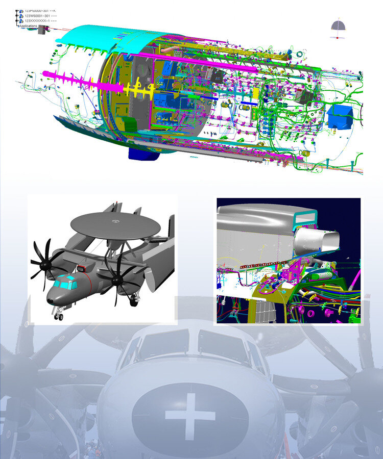
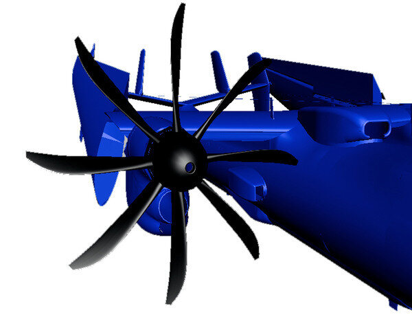
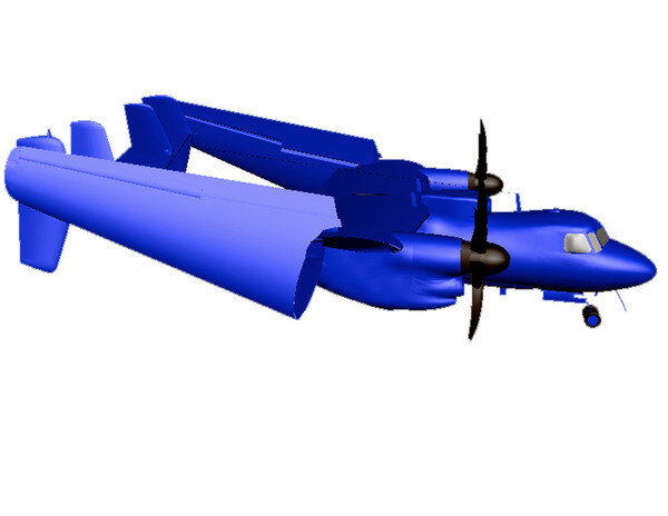
Automotive & Aerospace Design
Engineering has always been a part of our life. I have always wanted to become a design engineer. Drafting is sort of a way to design in today’s world. Yet appreciate being the drafting board learn to draw lines control circles using tools waiting for technology advance. It has enlightened. It has been educating and given me an image that any computer-aided drafting cannot assist. It is a work of art. It is a work of art for engineers. To see how much work and effort was put in drawing yet a the same time using mathematics using analytics using science to craft something to help this world advance in its innovation. Now today, I look back at my drafts. It looks like a work of art. I plan to create more work of drafting and one day make an exhibit of it. What you see here in this Gallery is just a few examples of my work as I learned the art of drafting.
IoT - Early Years
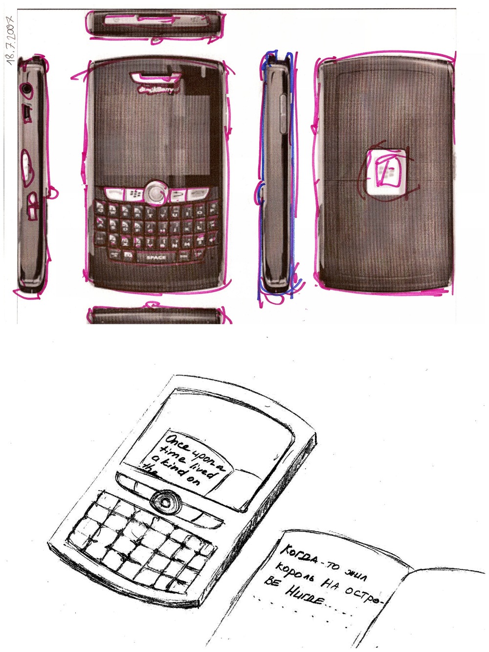


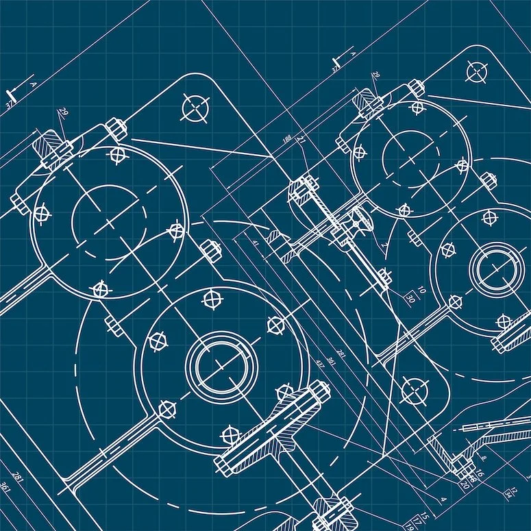
The Drafting Board

Drafting
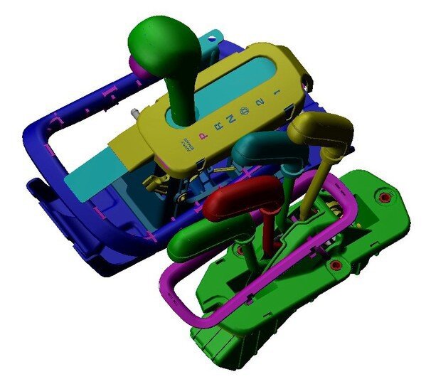
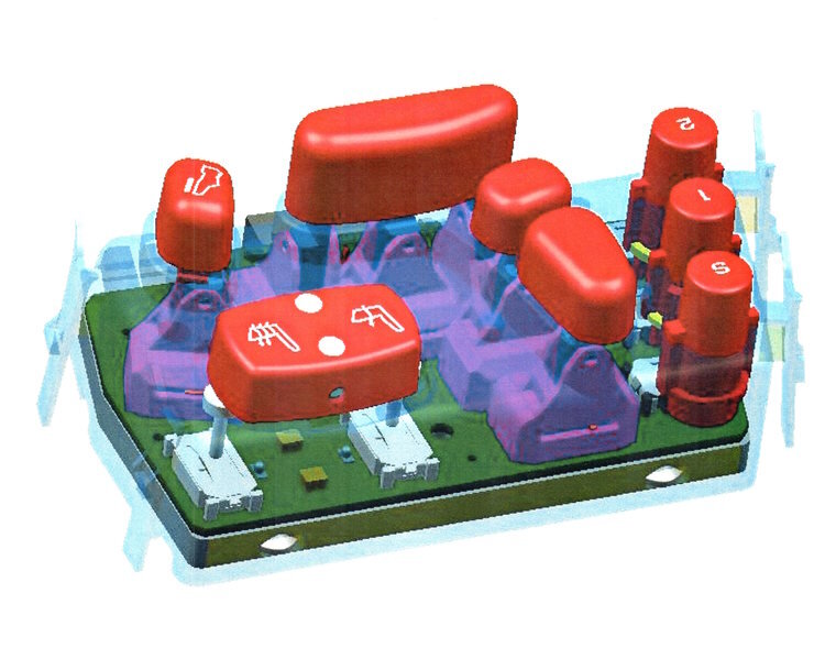
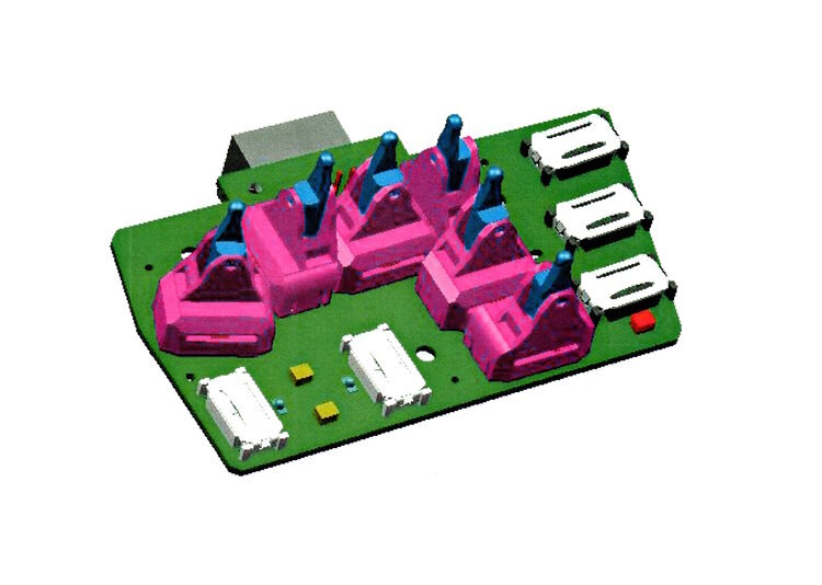
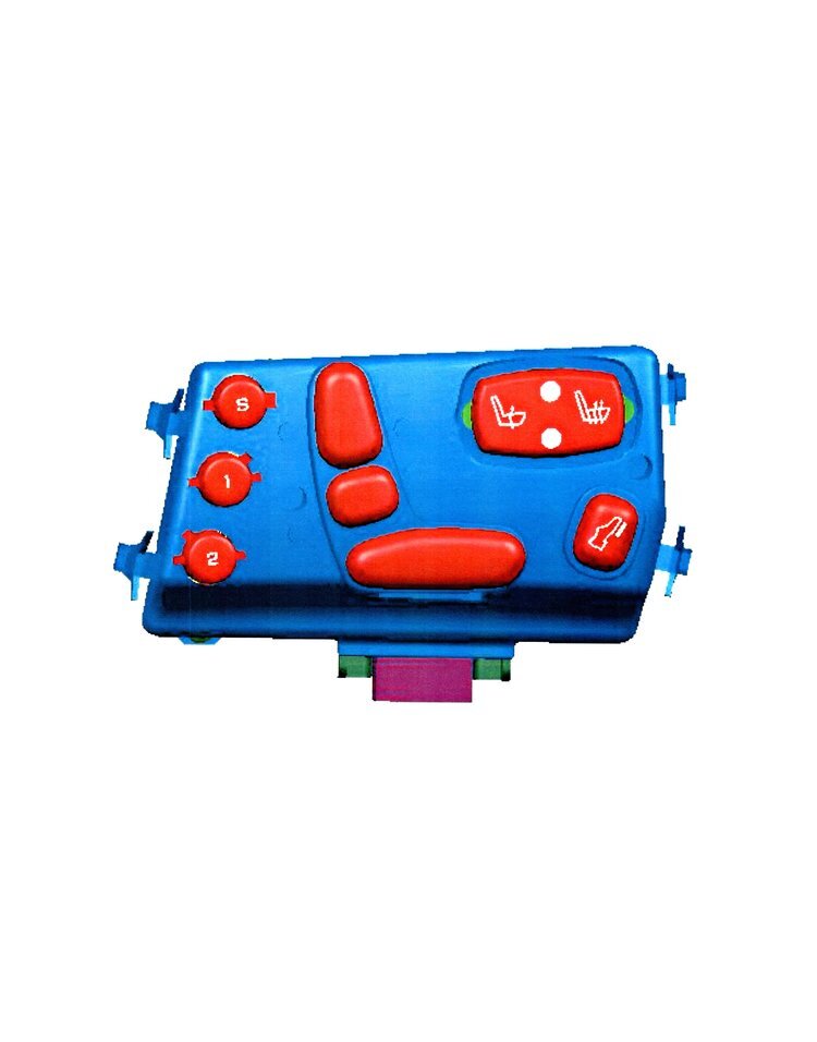
“”Electromechanical is being a mechanical process Vice actuated or controlled electronically especially being a transducer for converting electrical energy to mechanical energy – Merriam –Webster.
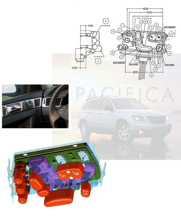
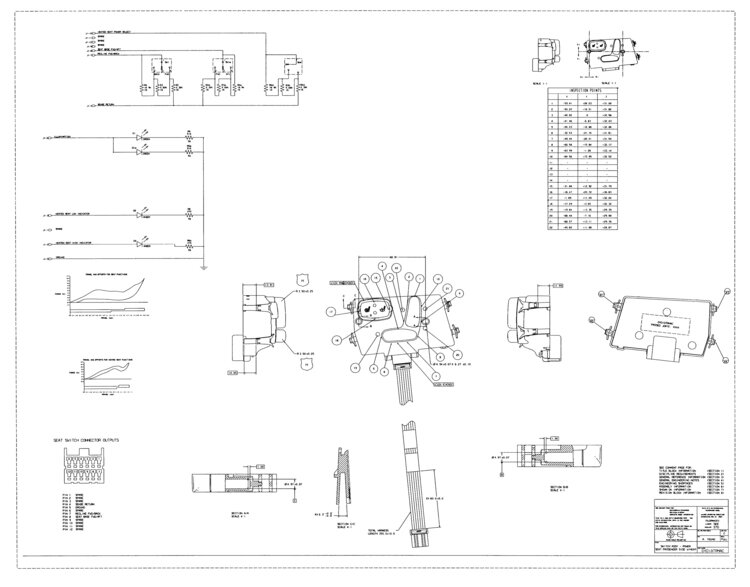
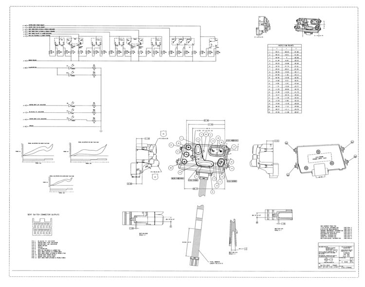
This is one of the first modules for controlling the driver and passenger seat when he comes to adjusting to the occupants by. Also, learning or developing how to heat the seats by touch of a button. As time went along Technology has enhance the seat module by the mere touch of a button even warming up the steering wheel.
A two-dimensional semiconductor (also known as 2D semiconductor) is a type of natural semiconductor with thicknesses on the atomic scale. The rising research attention towards 2D semiconductors started with a discovery by Geim and Novoselov et al. in 2004,[1] when they reported a new semiconducting material graphene, a flat monolayer of carbon atoms arranged in a 2D honeycomb lattice. A 2D monolayer semiconductor is significant because it exhibits stronger piezoelectric coupling than traditionally employed bulk forms, which enables 2D materials applications in new electronic components used for sensing and actuating.[2] In this emergent field of research in solid-state physics, the main focus is currently on designing nanoelectronic components by the use of graphene as electrical conductor, hexagonal boron nitride as electrical insulator, and a transition metal dichalcogenide as semiconductor.[3] - Wikipedia
Geometric Dimensioning and Tolerancing (GD&T) is a system for defining and communicating engineering tolerances. It uses a symbolic language on engineering drawings and computer-generated three-dimensional solid models that explicitly describes nominal geometry and its allowable variation. It tells the manufacturing staff and machines what degree of accuracy and precision is needed on each controlled feature of the part. GD&T is used to define the nominal (theoretically perfect) geometry of parts and assemblies, to define the allowable variation in form and possible size of individual features, and to define the allowable variation between features..
Dimensioning specifications define the nominal, as-modeled or as-intended geometry. One example is a basic dimension.
Tolerancing specifications define the allowable variation for the form and possibly the size of individual features, and the allowable variation in orientation and location between features. Two examples are linear dimensions and feature control frames using a datum reference (both shown above). -Wikipedia